Revision Notes on Solid and Electronic Device:-
- Thermoionic emission:- Thermionic emission is the phenomenon in which electrons are emitted by a metal contains free electrons which behave like the molecules of a perfect gas.
- Richardson Equation:-
I = AT1/2e-b/T
Here I is the thermionic current density in amp per sq meter. T is the temperature on kelvin scale, A and b being constants.
A = ne√k/2πm, b = e?/k
 Here, n is the number of electrons per unit volume, e is the charge on electron, m is the mass of electron, k is the Boltzmann’s constant and ? is the potential barrier of the metal.
- There are three types of energy bands in a solid viz.
(a)Valence energy band
(b)Conduction energy band
(c)Forbidden energy gap.
|
Valance Energy |
Forbidden Energy |
Conduction Energy Band |
|
In this band there are valence electrons. |
No electrons are found in this band |
In this band the electrons are rarely found |
|
This band may be partially or completely filled with electrons. |
This band is completely empty. |
This band is either empty or partially filled with electrons. |
|
In this band the electrons are not capable of gaining energy from external electric field. |
|
In this band the electrons can gain energy from electric field. |
|
The electrons in this band do not contribute to electric current. |
|
Electrons in this band contribute in this band contribute to electric current. |
|
In this band there are electrons of outermost orbit of atom which contribute in band formation. |
|
In this band there are electrons which are obtained on breaking the covalent bands. |
|
This is the band of maximum energy in which the electrons are always present. |
|
This is the band of minimum energy which is empty. |
|
This band can never be empty. |
|
This band can be empty. |
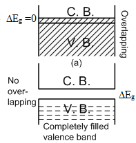
- Energy gap or Band gap (Eg):-

(a) The minimum energy which is necessary for shifting electrons from valence band to conduction band is defined as band gap (Eg)
(b) The forbidden energy gap between the valence band and the conduction band is known as band gap (Eg). i.e. Eg = Ec – Ev
(c) As there are energy levels f electrons in an atom, similarly there are three specific energy bands for the electrons in the crystal formed by these atoms as shown in the figure,

(d) Completely filled energy bands: The energy band, in which maximum possible numbers of electrons are present according to capacity is known as completely filled bank.
(e) Partially filled energy bands: The energy band, in which number of electrons present is less than the capacity of the band, is known as partially filled energy band.
(f) Electric conduction is possible only in those solids which have empty energy band or partially filled energy band.
- Various types of solids:-
On the basis of band structure of crystals, solids are divided in three categories.
(a) Insulators
(b) Semi-conductors
(c) Conductors.
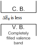
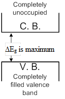
- Difference between Conductors, Semi-conductors and Insulators:-
|
S.No. |
Property |
Conductors |
Semi-conductors |
Insulators |
|
1. |
Electrical conductivity and its value |
Very high 10–7 mho/m |
Between those of conductors and insulators i.e. 10–7 mho/m to 10–13 mho/m |
Negligible 10–13 mho/m |
|
2. |
Resistivity and its value |
Negligible Less than 10–5 W-m |
Between those of conductors and insulators i.e. 10–5 W-m to 105 W-m |
Very high more than 105 W-m |
|
3. |
Band structure |
|
|
|
|
4. |
Energy gap and its value |
Zero or very small |
More that in con-ductors but less than that in insu-lators e.g. in Ge, ?Eg =0.72 eV is Si, ?Eg =1.1 eV in Ga As ?Eg =1.3 eV |
Very large e.g. in diamond ?Eg = 7 eV |
|
5. |
Current carriers and current flow |
Due to free electrons and very high |
Due to free electrons and holes more than that in insulators |
Due to free electrons but negligible. |
|
6. |
Number of current carriers (electrons or holes) at ordinary temperature |
Very high |
very low |
negligible |
|
7. |
Condition of valence band and conduction band at ordinary temperature |
The valence and conduction bands are completely filled or conduction band is some what empty (e.g. in Na) |
Valence band in somewhat empty and conduction band is somewhat filled |
Valence band is completely filled and conduction band is completely empty. |
|
8. |
Behaviour at 0 K |
Behaves like a superconductor. |
Behaves like an insulator |
Behaves like an insulator |
|
9. |
Temperature coefficient of resistance (a) |
Positive |
Negative |
Negative |
|
10. |
Effects of temperature on conductivity |
Conductivity decreases |
Conductivity increases |
Conductivity increases |
|
11. |
On increasing temperature the number of current carriers |
Decreases |
Increases |
Increases |
|
12. |
On mixing impurities their resistance |
Increases |
Decreases |
Remains unchanged |
|
13. |
Current flow in these takes place |
Easily |
Very slow |
Does not take place |
|
14. |
Examples |
Cu, Ag, Au, Na, Pt, Hg etc. |
Ge, Si, Ga, As etc. |
Wood, plastic, mica, diamond, glass etc. |
- The number of electrons or cotters is given by

i.e. on increasing temperature, the number of current carriers increases.
- The semiconductors are of two types.
(a) Intrinsic or pure semiconductors
(b) Extrinsic or dopes semiconductors
- Difference between Intrinsic and Extrinsic semiconductors:-
|
S.No. |
Intrinsic semiconductors |
Extrinsic semiconductors |
|
1. |
Pure Ge or Si is known as intrinsic semiconductor |
The semiconductor, resulting from mixing impurity in it, is known as extrinsic semiconductors. |
|
2. |
Their conductivity is low (because only one electron in 109 contribute) |
Their conductivity is high |
|
3. |
The number of free electrons (ni) in conduction band is equal to the number of holes (pi) in valence band. |
In this case ni is not equal to pi |
|
4. |
These are not practically used |
These are practically used |
|
5. |
In these the energy gap is very small |
In these the energy gap is more than that in pure semiconductors. |
|
6. |
In these the Fermi energy level lies in the middle of valence band and conduction |
In these the Fermi level shifts towards valence or conduction energy bands. |
- Child’s law:-
Ip = KVp3/2, K is the proportionality constant.
- Work function:-
Work function of a metal is the amount of energy required to pull an electron from the surface of metal to a distant position.
- Diode:-
It is a vacuum tube containing two electrodes, an emitter and a collector.
- Diode as a rectifier:-
Rectification is the process of converting the alternating current into a unidirectional current.
Rectification can be done by making use of a diode. A diode affecting rectification is said to be acting as a rectifier.
- Diode Resistance:-
(a) Static plate resistance:- (i) Rp = Vp/Ip (ii) Rp ∝ (Vp)-1/2 (iii) Rp ∝ (Ip)-1/3
(b) Dynamic plate resistance:- (i) rp = (ΔVp/ΔIp) (ii) rp∝Vp-1/2 (iii) rp∝Ip-1/2
-
Half-wave rectifier:- It is the type of rectification in which only one half of the input a.c. is translated into the output.
-
Full-wave rectifier:- A rectifier in which current flows through the load for both the halves of input a.c. is called half-wave rectifier.
-
Triode:- It is a vacuum tube containing three elements namely plate, filament and grid.
-
Triode constants:-
(a) Plate resistance (rp):- It is defined as the ratio between changes in plate potential keeping grid potential constant to the corresponding change in plate current.

(b) Mutual Inductance (gm):- (Trans-conductance):- It is defined as the ratio between change in plate current to the change in grid potential keeping plate potential constant required to bring about that change in current.

(c) Amplification factor (μ):- it is defined as the ratio between change in plate potential keeping grid potential constant to the change in grid potential keeping plate potential constant, in order to bring about same change in plate current.

(d) Relation between μ, rp and gm:-

(e) rp ∝Ip-1/3
(f) gm∝Ip1/3
- Triode as an amplifier:- Process of increasing the amplitude of the input signal is called amplification. A triode affecting an increase in the amplitude of a signal is said to be acting as an amplifier.
Voltage gain:- It is the ratio between the output voltage (voltage across the load resistance RL) to the signal voltage.
Voltage gain = V0/eg = μRL/RL+rp = μ/[1+(rp/RL)]
This indicates that the voltage gain depend upon the load resistance. For RL=∞, voltage gain is equal to the amplification factor.
(a) Ip = (μVg/RL+rp)
(b) A =μRL/RL+rp
(c) Amax = μ
(d) μ = A [1+(rp/RL)]
(e) A = μ/2 if RL = rp
- Cut off voltage:-
Vg = -(Vp/μ)
- Plate current equation:-
Ip = K[Vg+(Vp/μ)]3/2
- Triode as an oscillator:- A triode producing high frequency oscillating waves, of constant amplitude, is said to be acting as an oscillator.
Frequency of oscillation waves (f):- f = 1/2π√LC
Here L is the inductance and C is the capacitance.
- Majority charge carrier:-
(a) For N-type semiconductor:- electron
(b) For P-type semiconductor:- hole
- Electrical conductivity of semiconductors:-
Intrinsic semiconductors:-
(a) σ = e(neμe + nhμh)
Here, ne is the electron density, nh is the hole density,  is the electric mobilities and
  is the hole mobilities.
(b) 
Extrinsic semiconductor:-
(a) n-type:- σ = eneμe
(b) p-type:- σ = ennμn
- Transistor:-
 (a) IE = IC+IB (IB << IE, IB<<IC)
(b) Current gains:-
α = IC/IE, αac = ΔIC/ΔIE
β = IC/IB, βac = ΔIC/ΔIB
(c) Relation between α and β:-
α = β/[1+ β]
or
β = α/[1-α]
View courses by askIITians


Design classes One-on-One in your own way with Top IITians/Medical Professionals
Click Here Know More

Complete Self Study Package designed by Industry Leading Experts
Click Here Know More

Live 1-1 coding classes to unleash the Creator in your Child
Click Here Know More